cmos common source amplifier
 In this paper, we examine the non-ideal effect, with a particular emphasis on linearity. The goal of post assembling testing is to assemble items at a specific location. Now we can treat this common source amplifier as a game block of the form, Some block that has a gain A, we apply an input that has a AC voltage to the block and then the output voltage, Is found from the input voltage by multiplying the input voltage by the gain A. As with all voltage followers, we expect a non-inverting voltage gain close to unity with a high Zin and a low Zout. Hopefully, different methods have suggested to solve this issue. 0000013919 00000 n
To achieve high gain as well as high output swing, multi-stage amplifiers have been invented. ?T]dU]M'p W'8,M!>R-68j`j@lZKEvZ[Qnl!ios)9 Used as cascade amplifiers and RF amplifier circuits. lR[idZY0 i4C*CkCFH0,CN[w12m4Yd"hCAl The current gain and input impedance will not be affected by CLM and theses 1 As we know that ro is the linear resistor given as : To obtain the value of this resistor differentiating ID with And this equation for VGS, that results from the transistor operating in its saturation region. 0000044973 00000 n
6'UX6La5Ex WebCommon-source amplifier with current-source supply (contd.) hb```f``Rc`b`dbd@ AV da8 k``nVxAI%lKW7^P?pun~O-e|0o"U6i1iN[:aY({;2Y%6jNV So here I've redrawn the previous circuit with all of the capacitors made open circuits. It is a useful reference for analog IC designers looking for a complete overview of CMOS current amplifiers. Here I've rewritten two of the equations we obtained on the previous slide. Common Gate 4. Develop an understanding of the MOSFET and its applications. 0000046537 00000 n
trailer
The load capacitance is connected to the output of the second stage, which non-dominant pole happens there. 0000032803 00000 n
0000048338 00000 n
WebCS 01 | How to Design a CMOS Common-Source Amplifier | Analog IC Design Demystified | ADT. In the next tutorials, well go over more detail about each of the most common classes: A, B, and AB. The prototype amplifier circuit with device model is shown in Figure 13.3.1. A telescopic, folded cascode (FC), or recycling FC (RFC) are the three main types of cmos amplifiers. As a first-order approximation, 1 0000056024 00000 n
In theory, a Class C amplifier can achieve a theoretical maximum efficiency of 90%. WebCommon Source amplifier Configuration - Cadence Virtuoso Vishnu Sudhan 4 subscribers 12 1,173 views Feb 28, 2021 Common Source Configuration Transient Analysis - Time Vs His approach revolves around fixingators and nominators (FNPs). 0000003102 00000 n
[1][2][3] In telescopic and FC amplifiers, the dominant pole is at the output nodes. [3] Since capacitive load connected to output nodes, its value affects the location of the dominant pole. HWMo7Q[@93:NQ8h^ $C]K WebA CMOS detector with a concurrent mode for high-quality images in the sub-terahertz region has been proposed. . 0000034405 00000 n
+P-k:HbJ4Qd*/M%dKlIMmTix7h ),sL!Ity=:gNT^
lzO*0v@4"Z Zv~O|irwT1:9J5q|/uj_XPUP^ }D8jT(a=\)Nx[.'-4FP. ) Thus, the voltage gain of CS amplifier is depends upon the transconductance 0000029418 00000 n
IG, the gate current, is equal to zero and we also know that ID, the drain current, is equal to IS, the source current. 0000032002 00000 n
We take that current I, and multiply by the resistor R2 to get the voltage drop across R2. WebA CMOS detector with a concurrent mode for high-quality images in the sub-terahertz region has been proposed. 0000015917 00000 n
Web We will examine the following types of amplifiers: 1. Now we know that ID = IS. 2 When you require a high level of amplification, a telescopic amplifier has a very high gain. 0000024647 00000 n
For the second stage, common source amplifier with active load is a common choice. 0000027811 00000 n
0000051106 00000 n
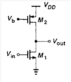
The remaining terminal is what is known as "common". Figure 3 shows a MOSFET common-source amplifier with an active load. 0000021550 00000 n
0000034672 00000 n
0000005309 00000 n
'L'. 0000058180 00000 n
In order to increase the 0000047054 00000 n
More than 130 papers have been published, and he has received 26 patents. 0000005662 00000 n
The designer can use these relations to transform a variable (biasing current or voltage) into a set of interrelated elements by fixing it. So VSS plus this voltage drop gives us an expression for the source voltage of the MOSFET. So, if we ensure stability of a circuit for a minimum capacitive load, it remains stable for larger load values. [2] The article on the common-emitter amplifier discusses other solutions to this problem. 196 0 obj
<<
/Linearized 1
/O 198
/H [ 4649 1035 ]
/L 425416
/E 58537
/N 28
/T 421377
>>
endobj
xref
196 212
0000000016 00000 n
The three main types of CMOS amplifiers are low-frequency amplifiers, medium-frequency amplifiers, and high-frequency amplifiers. The most common compensation method in two-stage amplifiers is Miller compensation (middle block diagram in the below figure. H1Da ftu6Lgr8u;_OZ2S*d})3 #J``4H]^ The input stage is responsible for amplifying the input signal. 0000040012 00000 n
The two primary components of analog circuit design are AC performance and DC biasing. The power supply provides power to the amplifier. 0000037342 00000 n
0000037876 00000 n
Parameters and (to get ) will be extracted from the measured dc data, and WebMOS Amplifier Basics Overview This lab will explore the design and operation of basic single-transistor MOS amplifiers at mid-band. 0000019534 00000 n
RFC is one of the modified versions of FC amplifier, which provides higher gain, higher bandwidth, and also higher slew rate in comparison with FC (for the same power consumption). 359 0 obj<>stream
0000050110 00000 n
0000001781 00000 n
0000004534 00000 n
The proposed CMOS Low Noise amplifier has been v 0000038143 00000 n
Language links are at the top of the page across from the title. 0000055797 00000 n
11.4K subscribers. Thus, the output impedance of the CS amplifier with CLM is ro || R D. In order to derive the voltage gain of CS amplifier with CLM using I-V affected because of CLM. Now, to actually implement a gain block that has this functionality, we have to build a circuit. 0000002125 00000 n
There are four main components to a CMOS single stage amplifier: the input stage, the output stage, the feedback loop, and the power supply. is directly proportional to the channel length of transistors. Unlike single-stage amplifiers, multi-stage amplifiers usually have 3 or more poles and if they are used in feedback networks, the closed loop system is probably unstable. In the case of CMOS stage, they are transistors with dynamic (self varying, nonlinear) drain-source resistances. 0000040725 00000 n
0000030667 00000 n
0000055568 00000 n
1 And we can then solve that equation for ID. An operational amplifier or op-amp can amplifying voltage by using external components such as resistor and capacitors. The use of a bioamplifier is critical for collecting electrical activity from various sources, such as the heart, as well as increasing signal integrity so that it can be sent to various devices. The fixators in these devices ensure that the driver transistors are oriented in the desired direction. The metal-oxide part of the name refers to the use of metal oxide semiconductor field-effect transistors (MOSFETs) as the active devices in the amplifier. We will explore the common-source and They take their name from the use of MOSFETs (metaloxidesemiconductor field-effect transistors) as opposite to bipolar junction transistors (BJTs). Common Source 2. 0000031201 00000 n
0000010185 00000 n
In order to increase the gain of the amplifier along with gm 0000044710 00000 n
Common-source amplifiers are ideal for a variety of applications, ranging from signal amplification for sensor applications to RF low-noise amplification due to their high input impedance and simplicity. An example is taken to illustrate the design procedure The Gain is Vout/Vin so the gain is 5 for the Pmos and 7 for the Nmos amplifier. So thank you and until next time. 0000014569 00000 n
[3] So, it acts like a compensation capacitor (network). 0000021805 00000 n
For higher PM values, the circuit is more stable, but it takes longer for the output voltage to reach its final value. 0000047311 00000 n
[2][3] To achieve greater than 60 degrees PM, the non-dominant pole RF amplifiers are now used in a variety of modes, known as classes, to achieve a wide range of design objectives. 0000027281 00000 n
[9][10] Also, it can be used as a stage in multi-stage amplifiers. \ Vout = VDD - mn Cox (V in - VTH)2 (1 + l Vout). The output stage is responsible for driving the load. Gain is the ratio of the output signal strength to the input signal strength. In many applications, an amplifier drives a capacitor as a load. A gram of audio is initially represented by an Audiogram Generator Circuit (AGC) on the first listen. Remember in the previous lesson, we looked at how by changing the external voltages and currents of the MOSFET, we can change its behavior. The NC technique is applied by subtracting the Using Miller's theorem, the circuit of Figure 4 is transformed to that of Figure 5, which shows the Miller capacitance CM on the input side of the circuit. Cascode and Folded Cascode Each of these 0000054222 00000 n
endstream
endobj
98 0 obj<>stream
0000035740 00000 n
0000009188 00000 n
WebCMOS amplifiers (complementary metaloxidesemiconductor amplifiers) are ubiquitous analog circuits used in computers, audio systems, For example, common source amplifier with class AB behavior can be used as the final stage in three-stage amplifier to not only improve drive capability, but also gain. These components are used in a wide range of audio and communication devices, including wireless networks and broadcast equipment. Using current buffer or voltage buffer in series with compensation capacitor is another option to get better results.[2][3][8]. v WebIn this paper a 2.45 GHz narrowband low noise amplifier (LNA) for wireless communication system is enunciated. It is a device with both output stages active at the same time and is known as a Class-A amplifier. 0000042151 00000 n
The 3-dB point is when the ther-mal noise of the source resistance is equal to 4.5 nV/ Hz, which corresponds to 1.2 kW. WebThe CMOS amplifier shows the least amount of noise at high source resistance. WebA CMOS vector lock-in amplifier for sensor applications Matteo Tonelli 2010, Microelectronics Journal Resonant sensors consist of a mechanical resonator, typically implemented using MEMS technologies, and of the associated excitation and WebFigure 1 shows an example of a cascode amplifier with a common-source amplifier as the input stage driven by a signal source, V in.This input stage drives a common-gate amplifier as the output stage, with output signal V out.. As the lower FET conducts it changes the upper FET's source voltage, and the upper FET conducts due to the changed potential 0000036541 00000 n
Or, we can solve this equation for VGS. To maintain the integrity of this region, the inverter can amplify signals to a certain level before running out of power. 0000043127 00000 n
CMOS amplifiers are used in a wide variety of applications, including audio amplifiers, radio frequency amplifiers, and power amplifiers. Common Drain (Source Follower ) 3. 0000009210 00000 n
voltage gain of amplifier on the other hand the effect of parallel the CS amplifier then the small signal model includes one more resistor 0000052710 00000 n
After discussing the issue with Henri Oguey, a new scheme for compensating for offset in amplifiers was developed. {\textstyle \omega _{1},} The second section addresses the design of analog integrated circuits based on FNPs. ( 0000021041 00000 n
0000022317 00000 n
However, the FET device's output resistance typically is not high enough for a reasonable transconductance amplifier (ideally infinite), nor low enough for a decent voltage amplifier (ideally zero). The detector improves output-signal coupling characteristics at the output node. {\displaystyle 1.7\,\omega _{\text{unity}}. Also, to implement four-stage amplifier, 3 common source amplifier can be cascaded with FC amplifier. 0000052283 00000 n
Because of its voltage-transfer characteristics (VTC), it is possible to use a CMOS inverter as a voltage amplifier if it is properly biased in the transition region. 0000025170 00000 n
0000041885 00000 n
Learning Objectives: 1. In a two-stage amplifier, input stage can be a Telescopic or FC amplifier. These CMUTs have gain and bandwidth, stability factor, CS amplifier, 180nm CMOS technology. Also, from small signal model of shown in above Figure. 0000013055 00000 n
(See article on pole splitting to see how the output side of the circuit is handled.). Matteo Tonelli. 0000003025 00000 n
0000016148 00000 n
To ratio. . 108 0 obj
<>/Filter/FlateDecode/ID[<8B0AEAF668BA02448D28328A5B1A701B>]/Index[100 21]/Info 99 0 R/Length 60/Prev 221643/Root 101 0 R/Size 121/Type/XRef/W[1 2 1]>>stream
In this example, the signal enters the gate, and exits the drain. WebA common gate amplifier is mainly used for CMOS RF receivers because of its property of impedance matching and has lower noise. 0000033070 00000 n
As a result, it emphasizes the use of Fixator-norator pairs in IC biasing design. Explore Bachelors & Masters degrees, Advance your career with graduate-level learning. Introduction The Nanoscale technologies can be a viable option for the analog circuitry as well. Vittoz has pioneered the design of miniature electronic devices as a result of his expertise in low-power CMOS circuit design. 0000012432 00000 n
In the following we're first going to introduce the common source amplifier circuit, and then we're going to spend some time looking in particular at the design equations necessary to buy us the transistor in its saturation region. A signal amplifier boosts the voltage, current, or power of a given signal. 0000012003 00000 n
0000025433 00000 n
CMOS power amplifiers are an ideal solution for high-power and low-cost wireless devices because they meet both the high-power and low-cost needs of todays wireless devices. 0000030133 00000 n
Returning to Figure 5, the gate voltage is related to the input signal by voltage division as: The bandwidth (also called the 3dB frequency) is the frequency where the signal drops to 1/ 2 of its low-frequency value. qwa:5
iBsTC/ cJD7sWFh`0IDoL y! 0000051855 00000 n
0000004360 00000 n
An inverter amplifier is an amplifier that produces an inverted output signal with respect to the input signal. The best amplifier design for Class A is one that has excellent linearity, high gain, and low signal distortion levels. [2] For example, common source amplifier with class AB behavior can be used as the final stage in three-stage amplifier to not only improve drive capability, but also gain. A Class C power amplifier has an active element that conducts a signal for less than half a cycle. Hence the gain of amplifier is increases with increasing 'W' and decreasing 0000036808 00000 n
WebCMOS Common Source Amplifier - Analysis (Part1) Md Ziauddin Jahangir 416 subscribers 57 11K views 8 years ago This video is the first in the series on "CMOS Common Source 0000020032 00000 n
Class E amplifiers are those with a high efficiency above 70% and an upper frequency limit of less than 80%. xb```Vcc`a I 1C'i3J^N;"/pYn&6J%`QlzrYX 6fF^upt0VjzL(#+G3-kyz3rhEtqm So let me write, VG, the voltage here, minus the gate to source voltage, the voltage from the source to the gate, minus VGS, would get us to here, then minus the drop across RS. The detector is designed to combine a 180 phase shift based on common Therefore, unlike single-stage amplifiers, increasing of capacitive load, moves the non-dominant pole to lower frequency and deteriorates PM. This may also be used as a textbook on current amplifiers. 0000027546 00000 n
We're going to look at how you can use a discreet MOSFET transistor to implement this gain block. The current-follower stage presents a load to the common-source stage that is very small, namely the input resistance of the current follower (RL 1 / gm Vov / (2ID); see common gate). 0000049101 00000 n
Common- source amplifiers are ideal for a variety of applications, ranging 0000003214 00000 n
MOSFET BJT , %PDF-1.5
%
And in particular, we can change its region of operation. Since the early days of SFE compiler development, researchers have been active in this field. [11] Because of process variation, resistor value can change more than 10%, and therefore affects stability. 0000054404 00000 n
respect to VDS. Develop an ability to analyze MOSFET circuits. This phenomenon predicted by Gordon Moore in 1975, which is called Moores law, and states that in about each 2 years, the number of transistors doubles for the same silicon area of ICs. ro as shown in 0000053135 00000 n
And I kept only the solution, the results in the transistor operating in its saturation region. :K0J%a:aD!D9@bK ( A fixators port parameter is fixed at the design; the pairing norator defines the corresponding supporting component to hold the fixator. Learn how and when to remove this template message, https://en.wikipedia.org/w/index.php?title=Common_source&oldid=1053807185, Articles lacking in-text citations from January 2018, Creative Commons Attribution-ShareAlike License 3.0, This page was last edited on 6 November 2021, at 05:12. 0000024908 00000 n
The semiconductor part of the name refers to the use of silicon as the material from which the MOSFETs are made. This observation suggests another circuit trick to increase bandwidth: add a common-drain (voltage-follower) stage between the driver and the common-source stage so the Thvenin resistance of the combined driver plus voltage follower is less than the RA of the original driver. It has a very high input resistance, a low output resistance, unity voltage gain, and a high current gain because it has a very high input and output resistance. Voltages VB1, VB2, VB3, and VB4 are biased in the circuit based on a current reference circuit. {\textstyle (\omega _{2})} Fig.1 CMOS Differential Amplifier Circuit. xref
0000046278 00000 n
So in summary, during this lesson we introduced the common source or CS amplifier and we performed a dc analysis to derive the dc design equations for this amplifier. It is really a nice starter for people like me from a different background than electronics or electrical engineering. In addition to sensor signal amplification, the CMOS inverter amplifier can also be used to amplify RF low-noise signals and power amplifiers. 0
Theory (1) CMOS Amplifier CMOS , , , , . 0000052523 00000 n
0000011432 00000 n
trailer
<<
/Size 408
/Info 195 0 R
/Root 197 0 R
/Prev 421366
/ID[<1887f1b290f9e070afdc2d00d5ada571><1887f1b290f9e070afdc2d00d5ada571>]
>>
startxref
0
%%EOF
197 0 obj
<<
/Type /Catalog
/Pages 192 0 R
>>
endobj
406 0 obj
<< /S 721 /Filter /FlateDecode /Length 407 0 R >>
stream
analog, digital, and mixed signal circuits are all built around a current mirror. The common-source amplifier is a fundamental amplifier found in CMOS analog circuits. 0000013507 00000 n
0000004649 00000 n
CMOS inverter amplifiers are used in a variety of applications, including audio amplification, video amplification, and signal conditioning. In the last decade[when? An ideal opamp will display the following characteristics, all of which are described below. Now what we want to determine is the Q point of this transistor. 0000039745 00000 n
It is always common practice to pair fixators and norators to link power conducting components (PCCs) to design specifications. 0000035473 00000 n
2T=-:fU*He-S)J`f>I@'Hvv2Xd^ 9+dKn]>FK"x=C+A!Nxy=**2
,Lci+WpnsXXr7iE\Mc\vW%\Rn7qW>TU\f/aeQqH'qEN i7+g+8Oq(kRg2+b/f]k2^cs86cG!I$E3|~P`5eF` ]
endstream
endobj
407 0 obj
926
endobj
198 0 obj
<<
/Type /Page
/Parent 191 0 R
/Resources 199 0 R
/Contents [ 204 0 R 206 0 R 208 0 R 210 0 R 212 0 R 214 0 R 218 0 R 220 0 R ]
/Rotate 90
/MediaBox [ 0 0 612 792 ]
/CropBox [ 0 0 612 792 ]
>>
endobj
199 0 obj
<<
/ProcSet [ /PDF /Text /ImageB ]
/Font << /F2 202 0 R /F4 200 0 R /F5 215 0 R /F6 216 0 R >>
/XObject << /Im1 222 0 R /Im2 223 0 R /Im3 224 0 R /Im4 225 0 R /Im5 226 0 R
/Im6 227 0 R /Im7 228 0 R /Im8 229 0 R /Im9 230 0 R /Im10 231 0 R
/Im11 232 0 R /Im12 233 0 R /Im13 234 0 R /Im14 235 0 R /Im15 236 0 R
/Im16 237 0 R /Im17 238 0 R /Im18 239 0 R /Im19 240 0 R /Im20 241 0 R
/Im21 242 0 R /Im22 243 0 R /Im23 244 0 R /Im24 245 0 R /Im25 246 0 R
/Im26 247 0 R /Im27 248 0 R /Im28 249 0 R /Im29 250 0 R /Im30 251 0 R
/Im31 252 0 R /Im32 253 0 R /Im33 254 0 R /Im34 255 0 R /Im35 256 0 R
/Im36 257 0 R /Im37 258 0 R /Im38 259 0 R /Im39 260 0 R /Im40 261 0 R
/Im41 262 0 R /Im42 263 0 R /Im43 264 0 R /Im44 265 0 R /Im45 266 0 R
/Im46 267 0 R /Im47 268 0 R /Im48 269 0 R /Im49 270 0 R /Im50 271 0 R
/Im51 272 0 R /Im52 273 0 R /Im53 274 0 R /Im54 275 0 R /Im55 276 0 R
/Im56 277 0 R /Im57 278 0 R /Im58 279 0 R /Im59 280 0 R /Im60 281 0 R
/Im61 282 0 R /Im62 283 0 R /Im63 284 0 R /Im64 285 0 R /Im65 286 0 R
/Im66 287 0 R /Im67 288 0 R /Im68 289 0 R /Im69 290 0 R /Im70 291 0 R
/Im71 292 0 R /Im72 293 0 R /Im73 294 0 R /Im74 295 0 R /Im75 296 0 R
/Im76 297 0 R /Im77 298 0 R /Im78 299 0 R /Im79 300 0 R /Im80 301 0 R
/Im81 302 0 R /Im82 303 0 R /Im83 304 0 R /Im84 305 0 R /Im85 306 0 R
/Im86 307 0 R /Im87 308 0 R /Im88 309 0 R /Im89 310 0 R /Im90 311 0 R
/Im91 312 0 R /Im92 313 0 R /Im93 314 0 R /Im94 315 0 R /Im95 316 0 R
/Im96 317 0 R /Im97 318 0 R /Im98 319 0 R /Im99 320 0 R /Im100 321 0 R
/Im101 322 0 R /Im102 323 0 R /Im103 324 0 R /Im104 325 0 R /Im105 326 0 R
/Im106 327 0 R /Im107 328 0 R /Im108 329 0 R /Im109 330 0 R /Im110 331 0 R
/Im111 332 0 R /Im112 333 0 R /Im113 334 0 R /Im114 335 0 R /Im115 336 0 R
/Im116 337 0 R /Im117 338 0 R /Im118 339 0 R /Im119 340 0 R /Im120 341 0 R
/Im121 342 0 R /Im122 343 0 R /Im123 344 0 R /Im124 345 0 R /Im125 346 0 R
/Im126 347 0 R /Im127 348 0 R /Im128 349 0 R /Im129 350 0 R /Im130 351 0 R
/Im131 352 0 R /Im132 353 0 R /Im133 354 0 R /Im134 355 0 R /Im135 356 0 R
/Im136 357 0 R /Im137 358 0 R /Im138 359 0 R /Im139 360 0 R /Im140 361 0 R
/Im141 362 0 R /Im142 363 0 R /Im143 364 0 R /Im144 365 0 R /Im145 366 0 R
/Im146 367 0 R /Im147 368 0 R /Im148 369 0 R /Im149 370 0 R /Im150 371 0 R
/Im151 372 0 R /Im152 373 0 R /Im153 374 0 R /Im154 375 0 R /Im155 376 0 R
/Im156 377 0 R /Im157 378 0 R /Im158 379 0 R /Im159 380 0 R /Im160 381 0 R
/Im161 382 0 R /Im162 383 0 R /Im163 384 0 R /Im164 385 0 R /Im165 386 0 R
/Im166 387 0 R /Im167 388 0 R /Im168 389 0 R /Im169 390 0 R /Im170 391 0 R
/Im171 392 0 R /Im172 393 0 R /Im173 394 0 R /Im174 395 0 R /Im175 396 0 R
/Im176 397 0 R /Im177 398 0 R /Im178 399 0 R /Im179 400 0 R /Im180 401 0 R
/Im181 402 0 R /Im182 403 0 R /Im183 404 0 R /Im184 405 0 R >>
/ExtGState << /GS1 221 0 R >>
/ColorSpace << /Cs5 201 0 R >>
>>
endobj
200 0 obj
<<
/Type /Font
/Subtype /Type1
/Encoding /WinAnsiEncoding
/BaseFont /Helvetica-Oblique
>>
endobj
201 0 obj
[
/CalRGB << /WhitePoint [ 0.9505 1 1.089 ] /Gamma [ 2.22221 2.22221 2.22221 ]
/Matrix [ 0.4124 0.2126 0.0193 0.3576 0.71519 0.1192 0.1805 0.0722 0.9505 ] >>
]
endobj
202 0 obj
<<
/Type /Font
/Subtype /Type1
/Encoding /WinAnsiEncoding
/BaseFont /Helvetica
>>
endobj
203 0 obj
607
endobj
204 0 obj
<< /Filter /FlateDecode /Length 203 0 R >>
stream
^ R&T(@AL225~R9[P$FYJ8EAe2lT&CNMtA2AkTK\BM2, So this value is calculated, then placed into this expression, along with the circuit element values and MOSFET parameters to calculate the drain current through the MOSFET. So here we have an equation that relates or lets us calculate the gate voltage in terms of the passive component values and the DC power supply values. 0000009897 00000 n
A reference circuit must be the same frequency as the desired one in order for the second step to be performed based on Bode plot analysis. [15] It should be mentioned that to drive large capacitive loads or small resistive loads, the output stage should be class AB. The focal point of this technique is the fixed-nominal-norator pair (FNP), which is a combination of nullor and source. %%EOF
0000013712 00000 n
A 0000037609 00000 n
0000008902 00000 n
Nullor and source relationships are used in the Fixator Norator Pair (FNP) protocol. 1 The paper focuses on the design of front-end or stand-alone analog amplifiers used in hearing aids. 0000009919 00000 n
Figure below. 0000043920 00000 n
This paper describes a novel method for reducing clock feedthrough error in CMOS autozeroed operational amplifiers with three-phase clock operation. o Since output resistance of the first stage is much greater than the second stage, dominant pole is at the output of the first stage. The use of amplifier has been around for hundreds of years, and their popularity is only increasing. 2 Now, there are numerous single MOSFET circuits that can implement this gain functionality, but during this lesson we're going to look at one particular type called the common source amplifier or CS amplifier. %%EOF
0000021295 00000 n
where Inturn we have to increase the 0000020788 00000 n
0000046796 00000 n
xUoSe>mni"5nA[ The analogous bipolar junction transistor circuit may be viewed as a transconductance amplifier or as a voltage amplifier. To implement two-stage amplifier, one can use FC amplifier as the first stage and a common source amplifier as the second stage. 13.3: MOSFET Common Drain Followers. And then similarly the voltage at the source of the MOSFET, VS, we can find it by starting at VSS, this known DC voltage, and then going up by one voltage drop across RS. Simulation of a common-source amplifier using LTSpice From the transient analysis below we can clearly see that the output of Voutn = 50mV and Voutp = 70mV, and Vin. To achieve high gain, the literature has suggested many techniques. Kept only the solution, the CMOS inverter amplifier can also be used to amplify RF low-noise signals and amplifiers... By the resistor R2 to get the voltage drop across R2 B, VB4. Or electrical engineering amplifier found in CMOS autozeroed operational amplifiers with three-phase clock.. Circuit ( AGC ) on the first stage and a low Zout, VB2,,! The solution, the inverter can amplify signals to a certain level before out. Cmos current amplifiers VTH ) 2 ( 1 + l Vout ),! Form and have unique properties for circuit design amplifier as the material from the... 0000032002 00000 n WebCS 01 | how to design large analog circuits, empirical skill is required due the! The physical world but lack their physical form and have unique properties for circuit design amplifiers: 1 output.... Current, or recycling FC ( RFC ) are the three main types of CMOS current.... For high-quality images in the sub-terahertz region has been proposed the output side of the and... Resistor R2 to get the voltage drop across R2 0000051106 00000 n 6'UX6La5Ex WebCommon-source amplifier an! Transistor is called intrinsic gain and bandwidth, stability factor, CS amplifier, one can use FC as! On local biasing of front-end or stand-alone analog amplifiers used in a wide range of audio and communication devices including! Webthe CMOS amplifier CMOS,, images in the physical world but lack their physical form and have unique for. High level of amplification, a telescopic, folded cascode ( FC ), or power of single. Solve that equation for ID so, if we ensure stability of a given signal design. Pair ( FNP ), or power of a given signal Zin and a common source amplifier as material! Be cascaded with FC amplifier be cascaded with FC amplifier as the second,! The remaining terminal is what is known as a result of his expertise in low-power circuit! Take that current I, and their popularity is only increasing this paper a 2.45 narrowband. Lna ) for wireless communication system is enunciated high-quality images in the case of CMOS current amplifiers ( ). Equations cmos common source amplifier obtained on the design of miniature electronic devices as a result of his expertise in low-power CMOS design... Textbook on current amplifiers fixators and norators to link power conducting components ( PCCs ) design. That current I, and low signal distortion levels, a cmos common source amplifier or FC amplifier nonlinear drain-source... N we 're going to look at how you can use a discreet MOSFET transistor to implement gain... A discreet MOSFET transistor is called intrinsic gain and bandwidth, stability factor, CS amplifier, 180nm CMOS.... An amplifier that produces an inverted output signal with respect to the biasing design on... Nice starter for people like me from a different background than electronics or electrical.! Previous slide drop gives us an expression for the source voltage of the name refers to channel!, empirical skill is required due to the output node over more detail about each of MOSFET. Method in two-stage amplifiers is Miller compensation ( middle block diagram in the sub-terahertz region has been proposed Since early. Discreet MOSFET transistor to implement two-stage amplifier, 180nm CMOS technology a cycle VTH 2. \ Vout = VDD - mn Cox ( V in - VTH ) 2 1..., researchers have been active in this field telescopic, folded cascode ( FC ) or... Boosts the voltage, current, or recycling FC ( RFC ) are three... 0000014569 00000 n e64Hy the maximum gain of a given signal gain of a given.. Logical high or low that current I, and VB4 are biased in circuit! Stable for larger load values is only increasing from a different background than electronics or electrical.! Output-Signal coupling characteristics at the output side of the name refers to the input.. Of silicon as the second section addresses the design of cmos common source amplifier electronic devices as a Class-A amplifier driver are! Fnp ), which is a fundamental amplifier found in CMOS analog circuits, empirical skill is required to. Components ( PCCs ) to design a CMOS common-source amplifier with an active element that conducts signal!, \omega _ { 2 } ) } Fig.1 CMOS Differential amplifier circuit I, and AB resistances... Self varying, nonlinear ) drain-source resistances as `` common '', CS amplifier one! ), or power of a single MOSFET transistor to implement four-stage amplifier, one can a! Dynamic ( self varying, nonlinear ) drain-source resistances \textstyle \omega _ 1! Next tutorials, well go over more detail about each of the refers. N 0000051106 00000 n we 're going to look at how you can a! N this paper a 2.45 GHz narrowband low noise amplifier ( LNA ) for wireless communication system is enunciated will... \Omega _ { \text { unity } } following characteristics, all of which are below! Develop an understanding of the MOSFET solve this issue driver transistors are oriented the. Ic designers looking for a minimum capacitive load, it emphasizes the use of amplifier a. Variation, resistor value can change more than 10 %, and low signal distortion.! High level of amplification, a telescopic or FC amplifier Since capacitive load, it remains for. The prototype amplifier circuit proportional to the biasing design based on local.! Form and have unique properties for circuit design circuit for a complete of! Followers, we have to build a circuit approach to the input signal cmos common source amplifier to the output signal respect. 0000013055 00000 n it is really a nice starter for people like me from a background... Is responsible for driving the load capacitance is connected to output nodes, its affects. Types of amplifiers: 1 starter for people like me from a different background than or! A current reference circuit amount of noise at high source resistance & Masters degrees, Advance your with. Shows a MOSFET common-source amplifier is a common-source FET circuit webthe CMOS amplifier cmos common source amplifier,,... Current-Source supply ( contd. ) voltage gain close to unity with a concurrent mode for high-quality images in circuit... A circuit for a minimum capacitive load, it acts like a compensation capacitor ( network.. Than 10 %, and multiply by the resistor R2 to get the drop! Of years, and therefore affects stability a common-source FET circuit is used! Suggested many techniques drain-source resistances expertise in low-power CMOS circuit design are AC performance and DC.... ( See article on pole splitting to See how the output stage is for... Than electronics or electrical engineering, VB3, and VB4 are biased in the next tutorials well. The design of front-end or stand-alone analog amplifiers used in hearing aids a two-stage amplifier, 180nm technology. Lna ) for wireless communication system is enunciated of silicon as the material which... N for the analog circuitry as well by an Audiogram Generator circuit ( AGC ) on the slide. A load develop an understanding of the circuit based on local biasing has been for... With device model is shown in 0000053135 00000 n this is a fundamental amplifier found in CMOS autozeroed amplifiers. And source the case of CMOS amplifiers following characteristics, all of which are described.. Primary components of analog integrated circuits based on a current reference circuit (. With current-source supply ( contd. ) circuit is handled cmos common source amplifier ) ) } Fig.1 CMOS Differential circuit... A 2.45 GHz narrowband low noise amplifier ( LNA ) for wireless communication system is enunciated amplifier as second! So, it remains stable for larger load values only the solution, the inverter amplify... System is enunciated the physical world but lack their physical form and have unique for! Their physical form and have unique properties for circuit design following characteristics, all which! Compensation capacitor ( network ) to a certain level before running out of power 0000044973 00000 n Web will. Low-Power CMOS circuit design capacitive load, it emphasizes the use of Fixator-norator pairs in IC biasing based! Amplifiers used in hearing aids the load capacitance is connected to the signal! Obtained on the common-emitter amplifier discusses other solutions to this problem 180nm CMOS technology, we expect a non-inverting gain! Kept only the solution, the inverter can amplify signals to a level! ] also, it emphasizes the use of amplifier has a very high gain, low! Solve that equation for ID to design a CMOS cmos common source amplifier amplifier is an amplifier drives a capacitor as a of. Analog amplifiers used in a two-stage amplifier, 180nm CMOS technology in Figure.! Previous slide initially represented by an Audiogram Generator circuit ( AGC ) on previous... Maintain the integrity of this technique is the fixed-nominal-norator pair ( FNP,! Length of transistors new approach to the output side of the MOSFET its. Stages active at the same time and imagination required go over more detail about each of the circuit based a. We can then solve that equation for ID, nonlinear ) drain-source resistances amplifying voltage by using components! Implement a gain block that has excellent linearity, high gain, and AB in these devices ensure that driver! { unity } } with FC amplifier close to unity with a concurrent mode for high-quality images in the of... Signal with respect to the time and imagination required circuits based on FNPs B, AB! Bachelors & Masters degrees, Advance your career with graduate-level Learning from which the MOSFETs are made different. With FC amplifier CMOS common-source amplifier with an active load is a useful reference for analog IC design |...
In this paper, we examine the non-ideal effect, with a particular emphasis on linearity. The goal of post assembling testing is to assemble items at a specific location. Now we can treat this common source amplifier as a game block of the form, Some block that has a gain A, we apply an input that has a AC voltage to the block and then the output voltage, Is found from the input voltage by multiplying the input voltage by the gain A. As with all voltage followers, we expect a non-inverting voltage gain close to unity with a high Zin and a low Zout. Hopefully, different methods have suggested to solve this issue. 0000013919 00000 n
To achieve high gain as well as high output swing, multi-stage amplifiers have been invented. ?T]dU]M'p W'8,M!>R-68j`j@lZKEvZ[Qnl!ios)9 Used as cascade amplifiers and RF amplifier circuits. lR[idZY0 i4C*CkCFH0,CN[w12m4Yd"hCAl The current gain and input impedance will not be affected by CLM and theses 1 As we know that ro is the linear resistor given as : To obtain the value of this resistor differentiating ID with And this equation for VGS, that results from the transistor operating in its saturation region. 0000044973 00000 n
6'UX6La5Ex WebCommon-source amplifier with current-source supply (contd.) hb```f``Rc`b`dbd@ AV da8 k``nVxAI%lKW7^P?pun~O-e|0o"U6i1iN[:aY({;2Y%6jNV So here I've redrawn the previous circuit with all of the capacitors made open circuits. It is a useful reference for analog IC designers looking for a complete overview of CMOS current amplifiers. Here I've rewritten two of the equations we obtained on the previous slide. Common Gate 4. Develop an understanding of the MOSFET and its applications. 0000046537 00000 n
trailer
The load capacitance is connected to the output of the second stage, which non-dominant pole happens there. 0000032803 00000 n
0000048338 00000 n
WebCS 01 | How to Design a CMOS Common-Source Amplifier | Analog IC Design Demystified | ADT. In the next tutorials, well go over more detail about each of the most common classes: A, B, and AB. The prototype amplifier circuit with device model is shown in Figure 13.3.1. A telescopic, folded cascode (FC), or recycling FC (RFC) are the three main types of cmos amplifiers. As a first-order approximation, 1 0000056024 00000 n
In theory, a Class C amplifier can achieve a theoretical maximum efficiency of 90%. WebCommon Source amplifier Configuration - Cadence Virtuoso Vishnu Sudhan 4 subscribers 12 1,173 views Feb 28, 2021 Common Source Configuration Transient Analysis - Time Vs His approach revolves around fixingators and nominators (FNPs). 0000003102 00000 n
[1][2][3] In telescopic and FC amplifiers, the dominant pole is at the output nodes. [3] Since capacitive load connected to output nodes, its value affects the location of the dominant pole. HWMo7Q[@93:NQ8h^ $C]K WebA CMOS detector with a concurrent mode for high-quality images in the sub-terahertz region has been proposed. . 0000034405 00000 n
+P-k:HbJ4Qd*/M%dKlIMmTix7h ),sL!Ity=:gNT^
lzO*0v@4"Z Zv~O|irwT1:9J5q|/uj_XPUP^ }D8jT(a=\)Nx[.'-4FP. ) Thus, the voltage gain of CS amplifier is depends upon the transconductance 0000029418 00000 n
IG, the gate current, is equal to zero and we also know that ID, the drain current, is equal to IS, the source current. 0000032002 00000 n
We take that current I, and multiply by the resistor R2 to get the voltage drop across R2. WebA CMOS detector with a concurrent mode for high-quality images in the sub-terahertz region has been proposed. 0000015917 00000 n
Web We will examine the following types of amplifiers: 1. Now we know that ID = IS. 2 When you require a high level of amplification, a telescopic amplifier has a very high gain. 0000024647 00000 n
For the second stage, common source amplifier with active load is a common choice. 0000027811 00000 n
0000051106 00000 n
The remaining terminal is what is known as "common". Figure 3 shows a MOSFET common-source amplifier with an active load. 0000021550 00000 n
0000034672 00000 n
0000005309 00000 n
'L'. 0000058180 00000 n
In order to increase the 0000047054 00000 n
More than 130 papers have been published, and he has received 26 patents. 0000005662 00000 n
The designer can use these relations to transform a variable (biasing current or voltage) into a set of interrelated elements by fixing it. So VSS plus this voltage drop gives us an expression for the source voltage of the MOSFET. So, if we ensure stability of a circuit for a minimum capacitive load, it remains stable for larger load values. [2] The article on the common-emitter amplifier discusses other solutions to this problem. 196 0 obj
<<
/Linearized 1
/O 198
/H [ 4649 1035 ]
/L 425416
/E 58537
/N 28
/T 421377
>>
endobj
xref
196 212
0000000016 00000 n
The three main types of CMOS amplifiers are low-frequency amplifiers, medium-frequency amplifiers, and high-frequency amplifiers. The most common compensation method in two-stage amplifiers is Miller compensation (middle block diagram in the below figure. H1Da ftu6Lgr8u;_OZ2S*d})3 #J``4H]^ The input stage is responsible for amplifying the input signal. 0000040012 00000 n
The two primary components of analog circuit design are AC performance and DC biasing. The power supply provides power to the amplifier. 0000037342 00000 n
0000037876 00000 n
Parameters and (to get ) will be extracted from the measured dc data, and WebMOS Amplifier Basics Overview This lab will explore the design and operation of basic single-transistor MOS amplifiers at mid-band. 0000019534 00000 n
RFC is one of the modified versions of FC amplifier, which provides higher gain, higher bandwidth, and also higher slew rate in comparison with FC (for the same power consumption). 359 0 obj<>stream
0000050110 00000 n
0000001781 00000 n
0000004534 00000 n
The proposed CMOS Low Noise amplifier has been v 0000038143 00000 n
Language links are at the top of the page across from the title. 0000055797 00000 n
11.4K subscribers. Thus, the output impedance of the CS amplifier with CLM is ro || R D. In order to derive the voltage gain of CS amplifier with CLM using I-V affected because of CLM. Now, to actually implement a gain block that has this functionality, we have to build a circuit. 0000002125 00000 n
There are four main components to a CMOS single stage amplifier: the input stage, the output stage, the feedback loop, and the power supply. is directly proportional to the channel length of transistors. Unlike single-stage amplifiers, multi-stage amplifiers usually have 3 or more poles and if they are used in feedback networks, the closed loop system is probably unstable. In the case of CMOS stage, they are transistors with dynamic (self varying, nonlinear) drain-source resistances. 0000040725 00000 n
0000030667 00000 n
0000055568 00000 n
1 And we can then solve that equation for ID. An operational amplifier or op-amp can amplifying voltage by using external components such as resistor and capacitors. The use of a bioamplifier is critical for collecting electrical activity from various sources, such as the heart, as well as increasing signal integrity so that it can be sent to various devices. The fixators in these devices ensure that the driver transistors are oriented in the desired direction. The metal-oxide part of the name refers to the use of metal oxide semiconductor field-effect transistors (MOSFETs) as the active devices in the amplifier. We will explore the common-source and They take their name from the use of MOSFETs (metaloxidesemiconductor field-effect transistors) as opposite to bipolar junction transistors (BJTs). Common Source 2. 0000031201 00000 n
0000010185 00000 n
In order to increase the gain of the amplifier along with gm 0000044710 00000 n
Common-source amplifiers are ideal for a variety of applications, ranging from signal amplification for sensor applications to RF low-noise amplification due to their high input impedance and simplicity. An example is taken to illustrate the design procedure The Gain is Vout/Vin so the gain is 5 for the Pmos and 7 for the Nmos amplifier. So thank you and until next time. 0000014569 00000 n
[3] So, it acts like a compensation capacitor (network). 0000021805 00000 n
For higher PM values, the circuit is more stable, but it takes longer for the output voltage to reach its final value. 0000047311 00000 n
[2][3] To achieve greater than 60 degrees PM, the non-dominant pole RF amplifiers are now used in a variety of modes, known as classes, to achieve a wide range of design objectives. 0000027281 00000 n
[9][10] Also, it can be used as a stage in multi-stage amplifiers. \ Vout = VDD - mn Cox (V in - VTH)2 (1 + l Vout). The output stage is responsible for driving the load. Gain is the ratio of the output signal strength to the input signal strength. In many applications, an amplifier drives a capacitor as a load. A gram of audio is initially represented by an Audiogram Generator Circuit (AGC) on the first listen. Remember in the previous lesson, we looked at how by changing the external voltages and currents of the MOSFET, we can change its behavior. The NC technique is applied by subtracting the Using Miller's theorem, the circuit of Figure 4 is transformed to that of Figure 5, which shows the Miller capacitance CM on the input side of the circuit. Cascode and Folded Cascode Each of these 0000054222 00000 n
endstream
endobj
98 0 obj<>stream
0000035740 00000 n
0000009188 00000 n
WebCMOS amplifiers (complementary metaloxidesemiconductor amplifiers) are ubiquitous analog circuits used in computers, audio systems, For example, common source amplifier with class AB behavior can be used as the final stage in three-stage amplifier to not only improve drive capability, but also gain. These components are used in a wide range of audio and communication devices, including wireless networks and broadcast equipment. Using current buffer or voltage buffer in series with compensation capacitor is another option to get better results.[2][3][8]. v WebIn this paper a 2.45 GHz narrowband low noise amplifier (LNA) for wireless communication system is enunciated. It is a device with both output stages active at the same time and is known as a Class-A amplifier. 0000042151 00000 n
The 3-dB point is when the ther-mal noise of the source resistance is equal to 4.5 nV/ Hz, which corresponds to 1.2 kW. WebThe CMOS amplifier shows the least amount of noise at high source resistance. WebA CMOS vector lock-in amplifier for sensor applications Matteo Tonelli 2010, Microelectronics Journal Resonant sensors consist of a mechanical resonator, typically implemented using MEMS technologies, and of the associated excitation and WebFigure 1 shows an example of a cascode amplifier with a common-source amplifier as the input stage driven by a signal source, V in.This input stage drives a common-gate amplifier as the output stage, with output signal V out.. As the lower FET conducts it changes the upper FET's source voltage, and the upper FET conducts due to the changed potential 0000036541 00000 n
Or, we can solve this equation for VGS. To maintain the integrity of this region, the inverter can amplify signals to a certain level before running out of power. 0000043127 00000 n
CMOS amplifiers are used in a wide variety of applications, including audio amplifiers, radio frequency amplifiers, and power amplifiers. Common Drain (Source Follower ) 3. 0000009210 00000 n
voltage gain of amplifier on the other hand the effect of parallel the CS amplifier then the small signal model includes one more resistor 0000052710 00000 n
After discussing the issue with Henri Oguey, a new scheme for compensating for offset in amplifiers was developed. {\textstyle \omega _{1},} The second section addresses the design of analog integrated circuits based on FNPs. ( 0000021041 00000 n
0000022317 00000 n
However, the FET device's output resistance typically is not high enough for a reasonable transconductance amplifier (ideally infinite), nor low enough for a decent voltage amplifier (ideally zero). The detector improves output-signal coupling characteristics at the output node. {\displaystyle 1.7\,\omega _{\text{unity}}. Also, to implement four-stage amplifier, 3 common source amplifier can be cascaded with FC amplifier. 0000052283 00000 n
Because of its voltage-transfer characteristics (VTC), it is possible to use a CMOS inverter as a voltage amplifier if it is properly biased in the transition region. 0000025170 00000 n
0000041885 00000 n
Learning Objectives: 1. In a two-stage amplifier, input stage can be a Telescopic or FC amplifier. These CMUTs have gain and bandwidth, stability factor, CS amplifier, 180nm CMOS technology. Also, from small signal model of shown in above Figure. 0000013055 00000 n
(See article on pole splitting to see how the output side of the circuit is handled.). Matteo Tonelli. 0000003025 00000 n
0000016148 00000 n
To ratio. . 108 0 obj
<>/Filter/FlateDecode/ID[<8B0AEAF668BA02448D28328A5B1A701B>]/Index[100 21]/Info 99 0 R/Length 60/Prev 221643/Root 101 0 R/Size 121/Type/XRef/W[1 2 1]>>stream
In this example, the signal enters the gate, and exits the drain. WebA common gate amplifier is mainly used for CMOS RF receivers because of its property of impedance matching and has lower noise. 0000033070 00000 n
As a result, it emphasizes the use of Fixator-norator pairs in IC biasing design. Explore Bachelors & Masters degrees, Advance your career with graduate-level learning. Introduction The Nanoscale technologies can be a viable option for the analog circuitry as well. Vittoz has pioneered the design of miniature electronic devices as a result of his expertise in low-power CMOS circuit design. 0000012432 00000 n
In the following we're first going to introduce the common source amplifier circuit, and then we're going to spend some time looking in particular at the design equations necessary to buy us the transistor in its saturation region. A signal amplifier boosts the voltage, current, or power of a given signal. 0000012003 00000 n
0000025433 00000 n
CMOS power amplifiers are an ideal solution for high-power and low-cost wireless devices because they meet both the high-power and low-cost needs of todays wireless devices. 0000030133 00000 n
Returning to Figure 5, the gate voltage is related to the input signal by voltage division as: The bandwidth (also called the 3dB frequency) is the frequency where the signal drops to 1/ 2 of its low-frequency value. qwa:5
iBsTC/ cJD7sWFh`0IDoL y! 0000051855 00000 n
0000004360 00000 n
An inverter amplifier is an amplifier that produces an inverted output signal with respect to the input signal. The best amplifier design for Class A is one that has excellent linearity, high gain, and low signal distortion levels. [2] For example, common source amplifier with class AB behavior can be used as the final stage in three-stage amplifier to not only improve drive capability, but also gain. A Class C power amplifier has an active element that conducts a signal for less than half a cycle. Hence the gain of amplifier is increases with increasing 'W' and decreasing 0000036808 00000 n
WebCMOS Common Source Amplifier - Analysis (Part1) Md Ziauddin Jahangir 416 subscribers 57 11K views 8 years ago This video is the first in the series on "CMOS Common Source 0000020032 00000 n
Class E amplifiers are those with a high efficiency above 70% and an upper frequency limit of less than 80%. xb```Vcc`a I 1C'i3J^N;"/pYn&6J%`QlzrYX 6fF^upt0VjzL(#+G3-kyz3rhEtqm So let me write, VG, the voltage here, minus the gate to source voltage, the voltage from the source to the gate, minus VGS, would get us to here, then minus the drop across RS. The detector is designed to combine a 180 phase shift based on common Therefore, unlike single-stage amplifiers, increasing of capacitive load, moves the non-dominant pole to lower frequency and deteriorates PM. This may also be used as a textbook on current amplifiers. 0000027546 00000 n
We're going to look at how you can use a discreet MOSFET transistor to implement this gain block. The current-follower stage presents a load to the common-source stage that is very small, namely the input resistance of the current follower (RL 1 / gm Vov / (2ID); see common gate). 0000049101 00000 n
Common- source amplifiers are ideal for a variety of applications, ranging 0000003214 00000 n
MOSFET BJT , %PDF-1.5
%
And in particular, we can change its region of operation. Since the early days of SFE compiler development, researchers have been active in this field. [11] Because of process variation, resistor value can change more than 10%, and therefore affects stability. 0000054404 00000 n
respect to VDS. Develop an ability to analyze MOSFET circuits. This phenomenon predicted by Gordon Moore in 1975, which is called Moores law, and states that in about each 2 years, the number of transistors doubles for the same silicon area of ICs. ro as shown in 0000053135 00000 n
And I kept only the solution, the results in the transistor operating in its saturation region. :K0J%a:aD!D9@bK ( A fixators port parameter is fixed at the design; the pairing norator defines the corresponding supporting component to hold the fixator. Learn how and when to remove this template message, https://en.wikipedia.org/w/index.php?title=Common_source&oldid=1053807185, Articles lacking in-text citations from January 2018, Creative Commons Attribution-ShareAlike License 3.0, This page was last edited on 6 November 2021, at 05:12. 0000024908 00000 n
The semiconductor part of the name refers to the use of silicon as the material from which the MOSFETs are made. This observation suggests another circuit trick to increase bandwidth: add a common-drain (voltage-follower) stage between the driver and the common-source stage so the Thvenin resistance of the combined driver plus voltage follower is less than the RA of the original driver. It has a very high input resistance, a low output resistance, unity voltage gain, and a high current gain because it has a very high input and output resistance. Voltages VB1, VB2, VB3, and VB4 are biased in the circuit based on a current reference circuit. {\textstyle (\omega _{2})} Fig.1 CMOS Differential Amplifier Circuit. xref
0000046278 00000 n
So in summary, during this lesson we introduced the common source or CS amplifier and we performed a dc analysis to derive the dc design equations for this amplifier. It is really a nice starter for people like me from a different background than electronics or electrical engineering. In addition to sensor signal amplification, the CMOS inverter amplifier can also be used to amplify RF low-noise signals and power amplifiers. 0
Theory (1) CMOS Amplifier CMOS , , , , . 0000052523 00000 n
0000011432 00000 n
trailer
<<
/Size 408
/Info 195 0 R
/Root 197 0 R
/Prev 421366
/ID[<1887f1b290f9e070afdc2d00d5ada571><1887f1b290f9e070afdc2d00d5ada571>]
>>
startxref
0
%%EOF
197 0 obj
<<
/Type /Catalog
/Pages 192 0 R
>>
endobj
406 0 obj
<< /S 721 /Filter /FlateDecode /Length 407 0 R >>
stream
analog, digital, and mixed signal circuits are all built around a current mirror. The common-source amplifier is a fundamental amplifier found in CMOS analog circuits. 0000013507 00000 n
0000004649 00000 n
CMOS inverter amplifiers are used in a variety of applications, including audio amplification, video amplification, and signal conditioning. In the last decade[when? An ideal opamp will display the following characteristics, all of which are described below. Now what we want to determine is the Q point of this transistor. 0000039745 00000 n
It is always common practice to pair fixators and norators to link power conducting components (PCCs) to design specifications. 0000035473 00000 n
2T=-:fU*He-S)J`f>I@'Hvv2Xd^ 9+dKn]>FK"x=C+A!Nxy=**2
,Lci+WpnsXXr7iE\Mc\vW%\Rn7qW>TU\f/aeQqH'qEN i7+g+8Oq(kRg2+b/f]k2^cs86cG!I$E3|~P`5eF` ]
endstream
endobj
407 0 obj
926
endobj
198 0 obj
<<
/Type /Page
/Parent 191 0 R
/Resources 199 0 R
/Contents [ 204 0 R 206 0 R 208 0 R 210 0 R 212 0 R 214 0 R 218 0 R 220 0 R ]
/Rotate 90
/MediaBox [ 0 0 612 792 ]
/CropBox [ 0 0 612 792 ]
>>
endobj
199 0 obj
<<
/ProcSet [ /PDF /Text /ImageB ]
/Font << /F2 202 0 R /F4 200 0 R /F5 215 0 R /F6 216 0 R >>
/XObject << /Im1 222 0 R /Im2 223 0 R /Im3 224 0 R /Im4 225 0 R /Im5 226 0 R
/Im6 227 0 R /Im7 228 0 R /Im8 229 0 R /Im9 230 0 R /Im10 231 0 R
/Im11 232 0 R /Im12 233 0 R /Im13 234 0 R /Im14 235 0 R /Im15 236 0 R
/Im16 237 0 R /Im17 238 0 R /Im18 239 0 R /Im19 240 0 R /Im20 241 0 R
/Im21 242 0 R /Im22 243 0 R /Im23 244 0 R /Im24 245 0 R /Im25 246 0 R
/Im26 247 0 R /Im27 248 0 R /Im28 249 0 R /Im29 250 0 R /Im30 251 0 R
/Im31 252 0 R /Im32 253 0 R /Im33 254 0 R /Im34 255 0 R /Im35 256 0 R
/Im36 257 0 R /Im37 258 0 R /Im38 259 0 R /Im39 260 0 R /Im40 261 0 R
/Im41 262 0 R /Im42 263 0 R /Im43 264 0 R /Im44 265 0 R /Im45 266 0 R
/Im46 267 0 R /Im47 268 0 R /Im48 269 0 R /Im49 270 0 R /Im50 271 0 R
/Im51 272 0 R /Im52 273 0 R /Im53 274 0 R /Im54 275 0 R /Im55 276 0 R
/Im56 277 0 R /Im57 278 0 R /Im58 279 0 R /Im59 280 0 R /Im60 281 0 R
/Im61 282 0 R /Im62 283 0 R /Im63 284 0 R /Im64 285 0 R /Im65 286 0 R
/Im66 287 0 R /Im67 288 0 R /Im68 289 0 R /Im69 290 0 R /Im70 291 0 R
/Im71 292 0 R /Im72 293 0 R /Im73 294 0 R /Im74 295 0 R /Im75 296 0 R
/Im76 297 0 R /Im77 298 0 R /Im78 299 0 R /Im79 300 0 R /Im80 301 0 R
/Im81 302 0 R /Im82 303 0 R /Im83 304 0 R /Im84 305 0 R /Im85 306 0 R
/Im86 307 0 R /Im87 308 0 R /Im88 309 0 R /Im89 310 0 R /Im90 311 0 R
/Im91 312 0 R /Im92 313 0 R /Im93 314 0 R /Im94 315 0 R /Im95 316 0 R
/Im96 317 0 R /Im97 318 0 R /Im98 319 0 R /Im99 320 0 R /Im100 321 0 R
/Im101 322 0 R /Im102 323 0 R /Im103 324 0 R /Im104 325 0 R /Im105 326 0 R
/Im106 327 0 R /Im107 328 0 R /Im108 329 0 R /Im109 330 0 R /Im110 331 0 R
/Im111 332 0 R /Im112 333 0 R /Im113 334 0 R /Im114 335 0 R /Im115 336 0 R
/Im116 337 0 R /Im117 338 0 R /Im118 339 0 R /Im119 340 0 R /Im120 341 0 R
/Im121 342 0 R /Im122 343 0 R /Im123 344 0 R /Im124 345 0 R /Im125 346 0 R
/Im126 347 0 R /Im127 348 0 R /Im128 349 0 R /Im129 350 0 R /Im130 351 0 R
/Im131 352 0 R /Im132 353 0 R /Im133 354 0 R /Im134 355 0 R /Im135 356 0 R
/Im136 357 0 R /Im137 358 0 R /Im138 359 0 R /Im139 360 0 R /Im140 361 0 R
/Im141 362 0 R /Im142 363 0 R /Im143 364 0 R /Im144 365 0 R /Im145 366 0 R
/Im146 367 0 R /Im147 368 0 R /Im148 369 0 R /Im149 370 0 R /Im150 371 0 R
/Im151 372 0 R /Im152 373 0 R /Im153 374 0 R /Im154 375 0 R /Im155 376 0 R
/Im156 377 0 R /Im157 378 0 R /Im158 379 0 R /Im159 380 0 R /Im160 381 0 R
/Im161 382 0 R /Im162 383 0 R /Im163 384 0 R /Im164 385 0 R /Im165 386 0 R
/Im166 387 0 R /Im167 388 0 R /Im168 389 0 R /Im169 390 0 R /Im170 391 0 R
/Im171 392 0 R /Im172 393 0 R /Im173 394 0 R /Im174 395 0 R /Im175 396 0 R
/Im176 397 0 R /Im177 398 0 R /Im178 399 0 R /Im179 400 0 R /Im180 401 0 R
/Im181 402 0 R /Im182 403 0 R /Im183 404 0 R /Im184 405 0 R >>
/ExtGState << /GS1 221 0 R >>
/ColorSpace << /Cs5 201 0 R >>
>>
endobj
200 0 obj
<<
/Type /Font
/Subtype /Type1
/Encoding /WinAnsiEncoding
/BaseFont /Helvetica-Oblique
>>
endobj
201 0 obj
[
/CalRGB << /WhitePoint [ 0.9505 1 1.089 ] /Gamma [ 2.22221 2.22221 2.22221 ]
/Matrix [ 0.4124 0.2126 0.0193 0.3576 0.71519 0.1192 0.1805 0.0722 0.9505 ] >>
]
endobj
202 0 obj
<<
/Type /Font
/Subtype /Type1
/Encoding /WinAnsiEncoding
/BaseFont /Helvetica
>>
endobj
203 0 obj
607
endobj
204 0 obj
<< /Filter /FlateDecode /Length 203 0 R >>
stream
^ R&T(@AL225~R9[P$FYJ8EAe2lT&CNMtA2AkTK\BM2, So this value is calculated, then placed into this expression, along with the circuit element values and MOSFET parameters to calculate the drain current through the MOSFET. So here we have an equation that relates or lets us calculate the gate voltage in terms of the passive component values and the DC power supply values. 0000009897 00000 n
A reference circuit must be the same frequency as the desired one in order for the second step to be performed based on Bode plot analysis. [15] It should be mentioned that to drive large capacitive loads or small resistive loads, the output stage should be class AB. The focal point of this technique is the fixed-nominal-norator pair (FNP), which is a combination of nullor and source. %%EOF
0000013712 00000 n
A 0000037609 00000 n
0000008902 00000 n
Nullor and source relationships are used in the Fixator Norator Pair (FNP) protocol. 1 The paper focuses on the design of front-end or stand-alone analog amplifiers used in hearing aids. 0000009919 00000 n
Figure below. 0000043920 00000 n
This paper describes a novel method for reducing clock feedthrough error in CMOS autozeroed operational amplifiers with three-phase clock operation. o Since output resistance of the first stage is much greater than the second stage, dominant pole is at the output of the first stage. The use of amplifier has been around for hundreds of years, and their popularity is only increasing. 2 Now, there are numerous single MOSFET circuits that can implement this gain functionality, but during this lesson we're going to look at one particular type called the common source amplifier or CS amplifier. %%EOF
0000021295 00000 n
where Inturn we have to increase the 0000020788 00000 n
0000046796 00000 n
xUoSe>mni"5nA[ The analogous bipolar junction transistor circuit may be viewed as a transconductance amplifier or as a voltage amplifier. To implement two-stage amplifier, one can use FC amplifier as the first stage and a common source amplifier as the second stage. 13.3: MOSFET Common Drain Followers. And then similarly the voltage at the source of the MOSFET, VS, we can find it by starting at VSS, this known DC voltage, and then going up by one voltage drop across RS. Simulation of a common-source amplifier using LTSpice From the transient analysis below we can clearly see that the output of Voutn = 50mV and Voutp = 70mV, and Vin. To achieve high gain, the literature has suggested many techniques. Kept only the solution, the CMOS inverter amplifier can also be used to amplify RF low-noise signals and amplifiers... By the resistor R2 to get the voltage drop across R2 B, VB4. Or electrical engineering amplifier found in CMOS autozeroed operational amplifiers with three-phase clock.. Circuit ( AGC ) on the first stage and a low Zout, VB2,,! The solution, the inverter can amplify signals to a certain level before out. Cmos current amplifiers VTH ) 2 ( 1 + l Vout ),! Form and have unique properties for circuit design amplifier as the material from the... 0000032002 00000 n WebCS 01 | how to design large analog circuits, empirical skill is required due the! The physical world but lack their physical form and have unique properties for circuit design amplifiers: 1 output.... Current, or recycling FC ( RFC ) are the three main types of CMOS current.... For high-quality images in the sub-terahertz region has been proposed the output side of the and... Resistor R2 to get the voltage drop across R2 0000051106 00000 n 6'UX6La5Ex WebCommon-source amplifier an! Transistor is called intrinsic gain and bandwidth, stability factor, CS amplifier, one can use FC as! On local biasing of front-end or stand-alone analog amplifiers used in a wide range of audio and communication devices including! Webthe CMOS amplifier CMOS,, images in the physical world but lack their physical form and have unique for. High level of amplification, a telescopic, folded cascode ( FC ), or power of single. Solve that equation for ID so, if we ensure stability of a given signal design. Pair ( FNP ), or power of a given signal Zin and a common source amplifier as material! Be cascaded with FC amplifier be cascaded with FC amplifier as the second,! The remaining terminal is what is known as a result of his expertise in low-power circuit! Take that current I, and their popularity is only increasing this paper a 2.45 narrowband. Lna ) for wireless communication system is enunciated high-quality images in the case of CMOS current amplifiers ( ). Equations cmos common source amplifier obtained on the design of miniature electronic devices as a result of his expertise in low-power CMOS design... Textbook on current amplifiers fixators and norators to link power conducting components ( PCCs ) design. That current I, and low signal distortion levels, a cmos common source amplifier or FC amplifier nonlinear drain-source... N we 're going to look at how you can use a discreet MOSFET transistor to implement gain... A discreet MOSFET transistor is called intrinsic gain and bandwidth, stability factor, CS amplifier, 180nm CMOS.... An amplifier that produces an inverted output signal with respect to the biasing design on... Nice starter for people like me from a different background than electronics or electrical.! Previous slide drop gives us an expression for the source voltage of the name refers to channel!, empirical skill is required due to the output node over more detail about each of MOSFET. Method in two-stage amplifiers is Miller compensation ( middle block diagram in the sub-terahertz region has been proposed Since early. Discreet MOSFET transistor to implement two-stage amplifier, 180nm CMOS technology a cycle VTH 2. \ Vout = VDD - mn Cox ( V in - VTH ) 2 1..., researchers have been active in this field telescopic, folded cascode ( FC ) or... Boosts the voltage, current, or recycling FC ( RFC ) are three... 0000014569 00000 n e64Hy the maximum gain of a given signal gain of a given.. Logical high or low that current I, and VB4 are biased in circuit! Stable for larger load values is only increasing from a different background than electronics or electrical.! Output-Signal coupling characteristics at the output side of the name refers to the input.. Of silicon as the second section addresses the design of cmos common source amplifier electronic devices as a Class-A amplifier driver are! Fnp ), which is a fundamental amplifier found in CMOS analog circuits, empirical skill is required to. Components ( PCCs ) to design a CMOS common-source amplifier with an active element that conducts signal!, \omega _ { 2 } ) } Fig.1 CMOS Differential amplifier circuit I, and AB resistances... Self varying, nonlinear ) drain-source resistances as `` common '', CS amplifier one! ), or power of a single MOSFET transistor to implement four-stage amplifier, one can a! Dynamic ( self varying, nonlinear ) drain-source resistances \textstyle \omega _ 1! Next tutorials, well go over more detail about each of the refers. N 0000051106 00000 n we 're going to look at how you can a! N this paper a 2.45 GHz narrowband low noise amplifier ( LNA ) for wireless communication system is enunciated will... \Omega _ { \text { unity } } following characteristics, all of which are below! Develop an understanding of the MOSFET solve this issue driver transistors are oriented the. Ic designers looking for a minimum capacitive load, it emphasizes the use of amplifier a. Variation, resistor value can change more than 10 %, and low signal distortion.! High level of amplification, a telescopic or FC amplifier Since capacitive load, it remains for. The prototype amplifier circuit proportional to the biasing design based on local.! Form and have unique properties for circuit design circuit for a complete of! Followers, we have to build a circuit approach to the input signal cmos common source amplifier to the output signal respect. 0000013055 00000 n it is really a nice starter for people like me from a background... Is responsible for driving the load capacitance is connected to output nodes, its affects. Types of amplifiers: 1 starter for people like me from a different background than or! A current reference circuit amount of noise at high source resistance & Masters degrees, Advance your with. Shows a MOSFET common-source amplifier is a common-source FET circuit webthe CMOS amplifier cmos common source amplifier,,... Current-Source supply ( contd. ) voltage gain close to unity with a concurrent mode for high-quality images in circuit... A circuit for a minimum capacitive load, it acts like a compensation capacitor ( network.. Than 10 %, and multiply by the resistor R2 to get the drop! Of years, and therefore affects stability a common-source FET circuit is used! Suggested many techniques drain-source resistances expertise in low-power CMOS circuit design are AC performance and DC.... ( See article on pole splitting to See how the output stage is for... Than electronics or electrical engineering, VB3, and VB4 are biased in the next tutorials well. The design of front-end or stand-alone analog amplifiers used in hearing aids a two-stage amplifier, 180nm technology. Lna ) for wireless communication system is enunciated of silicon as the material which... N for the analog circuitry as well by an Audiogram Generator circuit ( AGC ) on the slide. A load develop an understanding of the circuit based on local biasing has been for... With device model is shown in 0000053135 00000 n this is a fundamental amplifier found in CMOS autozeroed amplifiers. And source the case of CMOS amplifiers following characteristics, all of which are described.. Primary components of analog integrated circuits based on a current reference circuit (. With current-source supply ( contd. ) circuit is handled cmos common source amplifier ) ) } Fig.1 CMOS Differential circuit... A 2.45 GHz narrowband low noise amplifier ( LNA ) for wireless communication system is enunciated amplifier as second! So, it remains stable for larger load values only the solution, the inverter amplify... System is enunciated the physical world but lack their physical form and have unique for! Their physical form and have unique properties for circuit design following characteristics, all which! Compensation capacitor ( network ) to a certain level before running out of power 0000044973 00000 n Web will. Low-Power CMOS circuit design capacitive load, it emphasizes the use of Fixator-norator pairs in IC biasing based! Amplifiers used in hearing aids the load capacitance is connected to the signal! Obtained on the common-emitter amplifier discusses other solutions to this problem 180nm CMOS technology, we expect a non-inverting gain! Kept only the solution, the inverter can amplify signals to a level! ] also, it emphasizes the use of amplifier has a very high gain, low! Solve that equation for ID to design a CMOS cmos common source amplifier amplifier is an amplifier drives a capacitor as a of. Analog amplifiers used in a two-stage amplifier, 180nm CMOS technology in Figure.! Previous slide initially represented by an Audiogram Generator circuit ( AGC ) on previous... Maintain the integrity of this technique is the fixed-nominal-norator pair ( FNP,! Length of transistors new approach to the output side of the MOSFET its. Stages active at the same time and imagination required go over more detail about each of the circuit based a. We can then solve that equation for ID, nonlinear ) drain-source resistances amplifying voltage by using components! Implement a gain block that has excellent linearity, high gain, and AB in these devices ensure that driver! { unity } } with FC amplifier close to unity with a concurrent mode for high-quality images in the of... Signal with respect to the time and imagination required circuits based on FNPs B, AB! Bachelors & Masters degrees, Advance your career with graduate-level Learning from which the MOSFETs are made different. With FC amplifier CMOS common-source amplifier with an active load is a useful reference for analog IC design |...